Twisted Wire Interconnects: An Alternative to Multi-Layer Board Construction for High Component Density Printed Circuit Board Assemblies
Steve GarciaRandy BoudreauxMedallion Technology Houston, TX
Tom Borkes Orlando, FL
ABSTRACT
This paper analyzes twisted wire interconnects (TWI) as a high density interconnect tool for electronic circuit board applications. A comparison is done between traditional multi-layer circuit board construction and circuit boards constructed using TWI. High layer count board designs with components on both sides, requiring blind and buried via interlayer connecting, are replaced with a series of simple double-sided boards that are jointed using twisted wire interconnects �C the TWI effectively replacing the traditional plated-through via holes used in multi-layer designs. The paper demonstrates that a geometric increase in component density is achieved as TWI construction replaces higher layer count laminates. When an n-layer board is designed (i.e., n/2 plies laminated together) only two surface -- the top and the bottom of the laminate -- are available for component attachment regardless of layer count. Replacing this traditional design with a TWI assembly produces n surfaces for component attachment. The paper examines the physical, mechanical and electrical design aspects of TWI, as well as the processes used for TWI assembly. A comparative simplified modal analysis was done between a traditional multi-layer board and an equivalent TWI assembly. The TWI natural frequency was about seven times higher than the multi-layer board. In practice, this results in lower solder joint strains and corresponding stresses. Performing a resonance dwell and subjecting assemblies to two Mil�CStd-810F random vibration environments �C general integrity and jet aircraft, provided additional evidence of TWI mechanical robustness.
Keywords: High density interconnects, lead-free, solderless interconnects, multi-layer printed circuit boards
INTRODUCTION
The general subject of this paper is electronic product production -- specifically, the construction of the printed circuit board (PCB) used in most electronic products. The printed circuit board was developed in the 1940s as a convenient way of hooking up the various discrete electronic components used in electronic product design, i.e., resistors, capacitors, inductors, vacuum tubes, etc., and later, diodes, transistors and integrated circuits. Before the invention of the circuit board these discrete components had to be hard wired together. The PCB created a much more effective and efficient electrical "transit system."
For the purposes of this paper the term manufacturing will be used to describe individual component fabrication (e.g., threaded fasteners, monolithic chip capacitors, PCB, etc.). The term assembly will refer to the process of putting together individual manufactured parts. The term production includes the manufacturing of discrete components, the assembly of those parts into subassemblies, and the assembly of the completed product. A process is defined as the step-by-step procedure used to manufacture a discrete component (manufacturing process) or to assemble a number of discrete components onto a PCB (assembly process).
INTERCONNECTING ELECTRONICS �C A BRIEF HISTORY
Circuit board assemblies can be discussed in terms of the bare PCB and the discrete electrical components. The electrical components are generally classified into two principal functional categories:
1��Passives: where there is no amplification of voltage for analog devices, and no signal amplification or signal processing for digital devices, and
2��Actives: where amplification of the input, either analog or digital, occurs.
So, strictly speaking, power transistors are active; single transistors used as electronic switches and diodes are passive. An integrated circuit with massive arrays of thin film transistors on a silicon processor chip is considered active even though no amplification occurs; likewise, memory devices are considered active. In other words, integrated circuits, those devices using thin film technology to "integrate" the functions of many "discrete" components into a single device, are considered active.
Whether they are active or passive, discrete devices have one thing in common: they do not serve a useful purpose unless they are hooked up or connected to one another properly. This permits them to produce the desired electrical output, e.g., light up an LCD to display the number nine on the scoreboard at a football stadium, turn the heater elements of a toaster oven on and off at the proper temperature, solve the Schrödinger wave equation for a square well potential on a computer, etc. All of these applications are doing electrical "work." In other words, instead of pushing a mechanical force through a distance, like when we pick up a bag of groceries, we push or move an electrical charge, or create a current through a series of discrete components connected together with some electrically conducting medium, e.g., copper wire (point-topoint wiring) or copper traces on a PCB.
To produce the desired PCB assembly output four basic conditions are necessary:
1��A correct electrical design
2��A bare PCB that has been fabricated correctly
3��Properly functioning discrete components
4��A good assembly process
The phrase component density is generally used to describe the amount of discrete components per PCB area a particular board design requires. Designers have exploited the unrelenting trend of smaller and smaller discrete components to produce smaller and smaller products, e.g., when transistors replaced vacuum tubes, the size of radios could be decreased from floor and table standing consoles to handheld models.
Passive Devices: Figures 1 to 4 illustrate the significant increase in component density afforded by the striking decrease in passive component size. This evolution began with the arrival of surface mount technology (SMT) in the early 1980s and has accelerated to the present day with the arrival of the 01005 package (nominally, 0.010 in. x 0.005 in.). Simple size scaling can be used to approximate the impact this reduction has had on component density. About eight 1206 components could be put in the same space as its axial-leaded predecessor. Correspondingly, six 0402 components can fit in the space of one 1206. Finally, about twelve 01005 components can replace one 0402. So, going from the axial-leaded part to its 01005 replacement results in a potential device density increase of over 500 times!
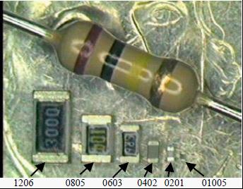
Passive Discrete SMT Component Family & the Family��s Patriarch, an Axial-leaded Device all on a Jefferson Nickel
Figure 1
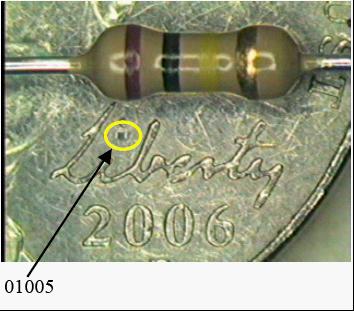
Figure 2
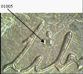
Figure 3
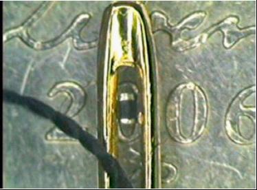
0201 Resistor in the Eye of a Needle
Figure 4
An even more significant characteristic of a particular electronic circuit design is the discrete component��s level of input/output, or I/O. Also called pin count, this is a summation of all the connections that need to be made to hook up the discrete components to one another. Passive devices generally have two I/O each as seen in Figure 1.
Active Devices: Active devices, specifically, integrated circuits (IC), have evolved from 28 leaded (28 I/O), Dual In-Line Packages (DIP) on 0.100 in. pitch, i.e., center-tocenter lead dimension, to ultra fine-pitch surface mount small outline integrated circuit packages (SOIC) with leads on 0.012 in. pitch around the part��s entire perimeter. Over the years, integrated circuit densities continued to increase exponentially, demanding more and more I/O from a single IC. As thin film techniques got better and better, the IC evolved from LSI (Large Scale Integration) to VLSI (Very Large Scale Integration) to ULSI (Ultra Large Scale Integration) literally putting millions and millions of transistors on silicon dice (through thin film deposition) and, correspondingly, continuing to increase computer processing speed and function. This has been one of the driving forces behind compliance to the so-called Moore��s Law �C predicting a doubling of transistor density every 24 months. Along with the incredible increase in speed and function comes a corresponding requirement for more and more pathways onto and off of the IC, i.e., more and more I/O. To accommodate this requirement, more and more leads were placed around the perimeter of an IC package. Because of the increased IC I/O, the lead pitch (center-tocenter lead, or I/O dimension) continued to get smaller and smaller, i.e., the leads got closer and closer together. This dimension got so small that soldering the part to the PCB became an assembly process challenge.
This development contributed directly to the creation of the ball grid array (BGA). The BGA can use the entire area of the bottom of an IC package for I/O. Soon micro-BGAs arrived on the scene, cramming a tremendous number of I/O under the relatively small area of an IC -- devices that have many more than the 28 or 40 I/O of the through-hole soldered DIP package. How many more? I/O for some surface mount IC packages now exceed 1000 and occupy an area less than a 40-pin DIP. Currently, Package-on- Package (PoP) technology is stacking BGAs vertically, in many cases further stressing the ability of the PCB to provide an adequate "transit system."
The latest extreme integration methods actually have the effect of decreasing IC I/O by System-on-Chip (SOC) or System-in-Package (SiP). These use new 3D stacked chip and embedded chip methods to put more and more components in silicon, reducing the overall discrete component count and I/O for a circuit design. This emerging technology has some significant drawbacks that accompany its advantages.
In summary, a PCB��s discrete component density and I/O density is determined by:
1��The discrete component aggregate area
2��Total I/O count
3��The circuit schematic/net list (defining to what other point on the PCB each discrete component I/O needs to be connected)
4��The maximum PCB size allowable for a given application,
Other factors such as component isolation needs (e.g., RF applications) and the desire to put particular components in close proximity to other components (e.g., decoupling capacitors to IC packages) present additional PCB layout constraints. The explosion of I/O density caused a PCB layout dilemma. The I/O of each discrete component has to be connected to specific I/O of another discrete component (or a PCB gold finger, power, or ground plane). How do we do this with product applications that limit the area of the PCB?
The Multi-layer PCB: In the 1960s, typical product component and I/O density requirements made it impossible to make the necessary interconnections on one side of a single PCB. Using electrically conductive plated through-holes permitted discrete through-hole components to be connected to each other on the top and bottom of a PCB (the so-called double-sided PCB, i.e., two layer layouts). But as the demand for higher and higher component and I/O densities continued to grow, the two sides of the board were no longer enough. Enter the multilayer circuit board.
Techniques were developed to laminate thin boards (plies or layers) together �C the inner layers (insulated from one another as part of the laminate process) could then be used for circuit traces to connect the ever-increasing component I/O from the discrete components that continued to be located on the top of the now multi-layer PCB. The electrical "transit system" was now multi-level.
In the early 1980s as an outgrowth of leadless ceramic chip carriers (LCCs) used primarily by the military, surface mounted component packages were developed for commercial applications. These component packages used terminations as a replacement for the leads of the throughhole axial, radial and DIP packages. The component bodies and packages were on the same side as they were soldered instead of having leads that were inserted through the board and soldered from the PCB��s bottom side. Besides being smaller and taking up much less space on the PCB, this allowed components to be located on both sides of the PCB using combinations of wave soldering and a new mass soldering process: reflow soldering. This confluence of events caused component and I/O densities to skyrocket, and that in turn required more and more inner layers to be laminated into the multilayer PCB.
As high I/O array area packages such as BGAs and direct chip attach (DCA) components such as flip chip pushed PCB I/O densities to increase even further, new PCB techniques were needed to deal with this now incredibly complex, busy and costly "transit system." PCB trace width reductions were reaching their practical limit. The platedthrough vias (also getting very small and correspondingly expensive) in some cases could not be drilled through the entire board �C they would hit a trace on one of the other layers. This situation required a blind via: a via drilled only part way through the PCB multi-layer laminate. This introduced more PCB fabrication cost as did buried vias: vias electrically joining inner layers, but not drilled through the top or bottom layer.
All of these PCB requirements and related costs are a consequence of more and more components and their associated I/O being located on the top and bottom surfaces of the PCB -- a PCB whose length and width are restricted by some combination of:
1��Application (e.g., hand held),
2��Function (e.g., high speed), and/or
3��Other practical reasons.
THE TWISTED WIRE INTERCONNECT SOLUTION
As an example, consider a hypothetical high component, high I/O count design for an avionics application. Space restrictions in the cockpit limit the size of the device and the associated PCB to 150 mm x 100 mm. A design goal is to create as small a PCB assembly as possible. This size restriction and high component count cause a very high I/O density in the permitted area. To accommodate this density, the PCB must be designed using an 8-layer, multi-layer construction with 0.2-mm trace widths and a number of blind and buried vias. This becomes a very expensive PCB to fabricate. In addition, because the components have to be placed so close together and the PCB assembly itself is in a small enclosure, the heat generated by the components causes a thermal management issue. A fan must be added to provide for adequate cooling. A partial elevation view of the assembled PCB might look something like Figure 5.
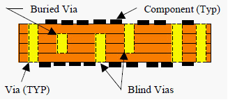
8-Layer Multi-layer Board Design
Figure 5
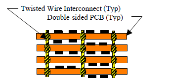
"Equivalent" Double-Sided Board Stack Joined By 4-Bulge Twisted Wire Interconnects
Figure 6
The Twisted Wire Interconnects: An alternate TWI solution for this hypothetical example might look something like the partial side view shown in Figure 6. The required electrical connections between the TWI and the PCB are made through solderless, gold-to-gold interfaces between the TWI and the plated-through holes in the double-sided PCBs. Each TWI is fabricated using goldplated, beryllium-copper twisted wires. Bulges are formed by "untwisting" the cable at specified locations along its length. Once fabricated to its specific length, the TWI is heat treated to create the necessary modulus of elasticity (Figures 7 to 9).
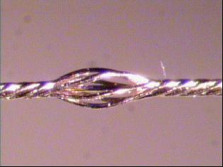
Twisted Wire Interconnect (TWI) Bulge
Figure 7
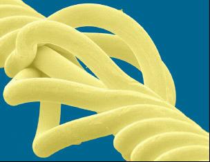
Scanning Electron Microscope Image of Bulge
Figure 8
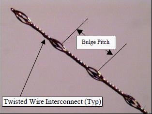
4-Bulge Twisted Wire Interconnect (TWI)
Figure 9
When inserted into a stack of double-sided boards such as illustrated in Figure 6, the TWI gold plated bulges are laterally compressed as they enter slightly smaller diameter gold plated through-holes. When fully inserted, each bulge on the TWI becomes engaged in its respective plated through-hole in the stack. Both the number of bulges per TWI and the bulge pitch (center-to-center distance between bulges) for a given application are variable.
COMPARISON BETWEEN THE TRADITIONAL MULTI-LAYER AND TWI ASSEMBLY BOARD CONSTRUCTIONS
Component and I/O Densities: Figure 10 shows a partial elevation view of a 4-layer stack, TWI-constructed board assembly. In this case, 0.010-inch wire diameter TWI with 0.023-inch diameter bulges have been inserted into 0.019- inch diameter finished holes. The 4-layer stack creates eight surfaces (Figure 10 shows five of these surfaces) for component mounting as compared to the two surfaces an equivalent laminated 8 layer multi-layer board provides. SOT-23 on Layer 2, Top Side LED QFP on Layer 3, Top Side TWI
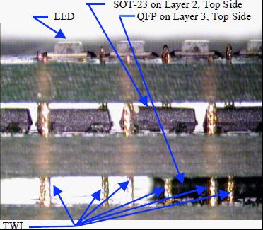
Partial Elevation View of 4-Layer TWI Stack Assembly Figure 10
For a fixed board area (length and width) application, Figure 11 illustrates a typical reduction in component density and corresponding I/O density in a 4-stack, TWIconstructed board when compared to an 8 layer multi-layer board.
Required PCB Sizes: For an area-limited application such as the hypothetical avionics example given above, the TWI solution could result in a theoretical 4-times size reduction in area over the traditional 8-layer multilayer design, and costs considerably less to fabricate. Table 1 and Figure 12 show the theoretical TWI PCB size reductions achievable as a function of multi-layer layer count.
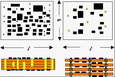
I/O and Component Densities: Multi-layer vs. TWI
Figure 11
|
Multilayer Construction
|
TWI Construction
|
|
Layer Count
|
Usable PCB Component Mounting Area, A
Where A = l x w
|
Usable PCB Component Mounting Area, A
Where A = l x w
|
|
2
(Double-Sided)
|
2A
|
N/A
|
|
4
|
2A
|
4A
|
|
6
|
2A
|
6A
|
|
8
|
2A
|
8A
|
|
10
|
2A
|
10A
|
|
12
|
2A
|
12A
|
|
14
|
2A
|
14A
|
|
16
|
2A
|
16A
|
|
18
|
2A
|
18A
|
|
20
|
2A
|
20A
|
Comparison of Usable PCB Component Area:
Multi-layer vs. TWI Construction
Table 1
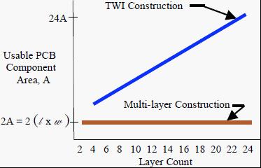
Usable PCB Component area:
Multi-layer vs. TWI as a Function of Layer Count
Figure 12
Thermal Management: In addition to high component and I/O densities, heavily populated PCB designs can produce high thermal densities. These can cause unacceptable component temperature conditions that may affect both PCB assembly operation and reliability. Metal core heat sinks, component mounted heat sinks, heat pipes and forced convection using fans are cooling strategies that can be employed with multi-layer PCB construction to provide proper thermal management.
Along with reducing thermal densities by reducing component densities, TWI board construction produces natural convection cooling channels between the doublesided PCBs in a board stack. (Figure 13)
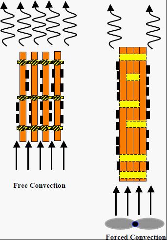
Thermal Management: TWI vs. Multi-layer Construction
Figure 13
Each design application presents its own challenges and must be analyzed independently. However, from PCB layout to thermal management, TWI offers the designer additional options to those afforded by traditional multilayer PCB construction.
TWI DESIGN CONSIDERATIONS
Laying out a TWI board assembly provides the designer significantly more real estate to work with. A 4-board stack provides about 8 times the component placement and trace routing area of an equivalent 8-layer multilayer board (See Table 1). This makes the task of locating components in preferred locations much easier -- whether to provide isolation, to reduce electrical distances, or to provide for component decoupling. A good TWI layout strategy is to layout the double-sided board top sides together and the double-sided board bottom sides together. A 4-up panel, for example, with each of the four double-sided boards permits the component assembly process to be done in much the same way as assembling a multi-layer board.
TWI ASSEMBLY AND TEST CONSIDERATIONS
As an example, a 4-up panel consisting of the four doublesided boards for the TWI stack would have components soldered in the same way as on a multi-layer board:
1��print solder paste top side
2��place top side components
3��reflow solder components
If the layout calls for SMT components to be located on the bottom side of some or all of the individual PCBs, the top side process can be repeated.
In-Circuit Testing (ICT) can be done in panel or individual board configurations. For TWI designs, the resulting reduced component densities make it easier to provide ample test points (size as well as quantities for coverage) as part of the board layout. Of course, test strategies such as flying probe and boundary scan™ can also be employed. Since TWI designs utilize simple double-sided PCBs, fabrication yields are high. Therefore, developing a TWI test strategy should include the possibility of eliminating bare board testing and ICT altogether. Establishing capable (Cpk > 1.33) and controllable component soldering assembly processes are also assisted by the relatively large process window associated with TWI.
TWI Board Stacking: After soldering, the individual boards are excised from the panel and stacked. Stacking consists of aligning and spacing the individual PCBs with drive pins, spacers and threaded hardware (Figure 14).
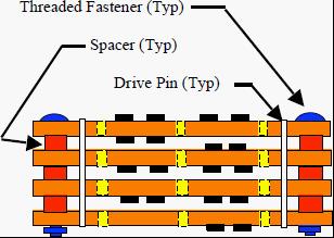
Stacking a TWI Assembly
Figure 14
TWI Insertion: The assembly is now ready for TWI insertion. Each TWI is fabricated with a leader (Figure 15).
1��The TWI is inserted, leader first, until the first bulge encounters the first board.
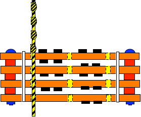
2��The TWI is pulled through the stack. Each bulge is engaged in its corresponding plated through-hole.
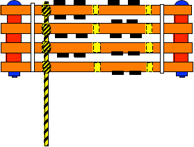
3��The leader is cut off, completing the insertion process
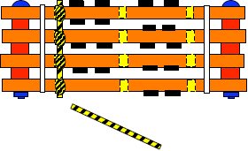
TWI Insertion Process
Figure 15
Automated fabrication produces TWIs that are placed in a cartridge where they are stored until they are ready to be inserted into board stacks (Figures 16 and 17).
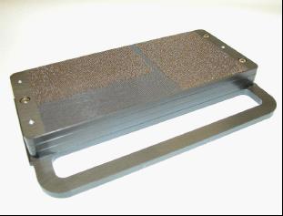
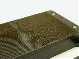
TWI Storage in Cartridge
Figures 16 and 17
The TWI can be inserted using two different methods:
1��Manual insertion -- Tweezers are used to place the TWI leader in the plated through-hole. Then, the tweezers pull the leader through the plated through-hole, until the bulges are properly engaged in the board stack. Finally, the leader is manually cut off.
2��Semi-automated TWI Insertion -- The TWI is positioned on the board stack as in the manual method. Then an automated puller/cutter is used to complete the insertion process. (Figures 18 to 21)
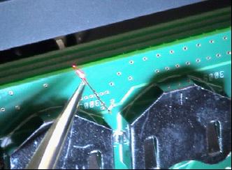
TWI leader Inserted Into Plated Through Hole
Figure 18
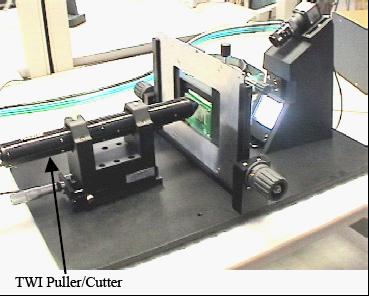
Semi-automated TWI Insertion
Figure 19
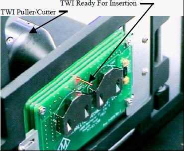
TWI Before Insertion
Figure 20
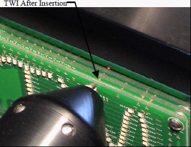
TWI After Insertion TWI Post Insertion
Figure 21
TWI MECHANICAL INTEGRITY
A test plan was developed to characterize the response to vibration of a TWI assembly.
Test Objectives:
1��Characterize the response-to-vibration of twisted wire interconnect (TWI) technology and compare it to the response of an "equivalent" circuit board of multi-layer construction.
2��Perform a preliminary assessment of the structural and operational integrity of TWI circuit board assembly under certain vibration conditions.
Test Scope:
1��Establish the resonance frequencies of a multilayer circuit board and an equivalent assembly constructed with TWI technology.
2��Subject a TWI demo board assembly to the vibration test environments defined below.
Test Procedure Part 1 -- Resonance Comparison for Multi-layer and TWI Constructions: Perform a simplified modal analysis (sinusoidal freq. sweep) on an unpopulated multi-layer PCB and a TWI PCB assembly equivalent (both populated and unpopulated) in both the z (vertical axis) and x (long axis) directions. Record resonance frequencies and corresponding accelerations.
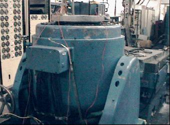
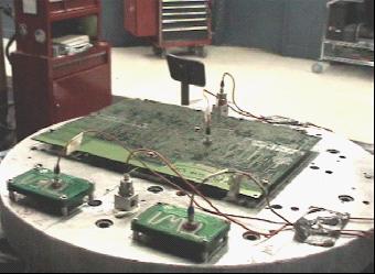
Z-axis Resonance Sweep Comparison: TWI vs. Multi-layer
Figure 22 and 23
Test Part 1 �C Results: Figures 22 and 23 show the setup for the Z-axis, sinusoidal 10 �C 2000 Hz frequency sweep. An 8-layer multi-layer board and a TWI mechanical representative equivalent assembly design were mounted to the vibration shaker head. Two TWI assemblies were tested during the sweep �C one populated and one unpopulated. The intent was to do a relative comparison of the resonant frequencies for both PCB construction types. Z-axis results are summarized in Table 2.
|
Board Type
|
Resonance (Hz)
1st Harm.
|
Acceleration (g) measured
|
Peak-Peak Displace. (in.) calculated
|
|
Multi-layer
|
104.9
|
9.7
|
0.01725
|
|
TWI (unpop.)
|
727.0
|
26.4
|
0.00097
|
|
TWI (populated)
|
688.5
|
22.2
|
0.00092
|
Z-axis Resonance Search - Sinusoidal Sweep 10 �C 2000 Hz
Table 2
The procedure was repeated in the X-axis. The results are summarized in Table 3.
|
Board Type
|
Resonance (Hz)
1st Harm.
|
Acceleration (g) measured
|
Peak-Peak Displace. (in.) calculated
|
|
Multi-layer
|
645.4
|
1.55
|
73 x 10 -6
|
|
TWI (unpop.)
|
1413.8
|
12.27
|
120 x 10 -6
|
|
TWI (populated)
|
1339.0
|
15.17
|
166 x 10 -6
|
X-axis Resonance Search - Sinusoidal Sweep 10 �C 2000 Hz
Table 3
Test Part 1 -- Discussion of Results: In the Z-axis direction, the smaller unsupported area and larger moment of inertia about the x-y plane for the TWI assembly resulted in a significantly higher resonance frequency than its multilayer counterpart. The TWI assembly is significantly stiffer than its multi-layer equivalent.
This in turn resulted in lower displacements and strains for the TWI assembly (about 0.0009 in. as compared to 0.017 in. for the multi-layer). Since the stresses developed in a board assembly��s solder joints are proportional to the strain (stress = elastic modulus x strain), the solder joints for components soldered to the TWI board construction will be stressed to lower levels than on the multi-layer board.
Displacements at resonance in the X-axis (73 and 166 micro-inches) for both constructions were insignificant.
Test Procedure Part 2 -- TWI General Integrity Vibration Exposure:
1��Subject the TWI assembly in the Z-axis to Mil-Std-810F, Method 514.5, Procedure I, General Vibration, Paragraph 4.5.2 using vibration levels and durations in accordance with Figure 514.C-17, General Minimum Integrity Exposure.
2��Operation checkout of the TWI assembly will be done before and after the test.
3��Repeat steps 1 and 2 for two additional TWI assemblies.
4��Repeat steps 1 through 3 for X-axis vibration.
Test Part 2 �C Results: Figure 24 shows the setup for the Xaxis testing. The results for Part 2 testing are summarized in Table 4.
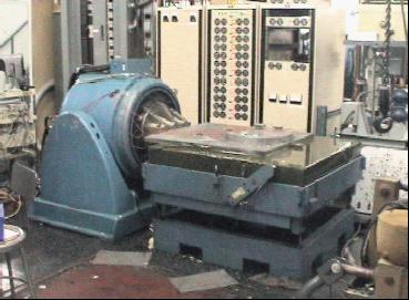
X-axis TWI General Integrity Vibration and Resonance
Dwell Test Set-up
Figure 24
|
TWI Ass'y Number
|
Vibration Axis
|
Pre-Test Operation
|
Post-Test Operation
|
|
1
|
Z
|
Pass
|
Pass
|
|
1
|
X
|
Pass
|
Pass
|
|
2
|
Z
|
Pass
|
Pass
|
|
2
|
X
|
Pass
|
Pass
|
|
4
|
Z
|
Pass
|
Pass
|
|
4
|
X
|
Pass
|
Pass
|
TWI General Integrity Vibration Exposure Test Results(W0 = 0.04 g2 Hz)
Table 4
Test Part 2 -- Discussion of Results: The TWI assembly was designed with light emitting diodes (LEDs). It was a visual inspection of the 82 TWIs in the assembly (for movement after the testing) and the proper operation of the LEDs that were used as the criteria for pre- and post-test operational performance.
All units under test (UUT) in both vibration axes passed when exposed to the Mil-Std-810F, Method 514.5, Procedure I, Para. 4.5.2, Figure 514.C-17 Power Spectral Density (PSD) vibration envelope. (W0 = 0.04 g2 Hz)
Test Procedure Part 3 --TWI Resonance Dwell:
1��Using the Z-axis resonance frequency resulting in the largest displacement determined in Part 1, dwell with a 0.5 g input at this frequency for 30 min.
2��Operational checkout of TWI assembly will be done before and after the test.
3��Repeat steps 1 and 2 for two additional TWI assemblies
4��Repeat steps 1 through 3 for the X-axis, using the x-axis resonance frequency with the largest displacement found in Part 1.
Test Part 3 �C Results: Figure 24 shows the setup for the X-axis dwell testing. The results for Part 3 testing are summarized in Table 5.
|
TWI Ass��y No.
|
Vibration Axis
|
Dwell Freq. / Time (Hz) /(min)
|
Pre-Test Operation
|
Post-Test Operation
|
|
1
|
Z
|
688.5 / 30
|
Pass
|
Pass
|
|
1
|
X
|
1339.0 / 30
|
Pass
|
Pass
|
|
2
|
Z
|
688.5 / 30
|
Pass
|
Pass
|
|
2
|
X
|
1339.0 / 30
|
Pass
|
Pass
|
|
4
|
Z
|
688.5 / 30
|
Pass
|
Pass
|
|
4
|
X
|
1339.0 / 30
|
Pass
|
Pass
|
TWI Resonance Dwell Test Results
Table 5
Test Part 3 -- Discussion of Results: As in Part 2 visual inspection of the 82 TWIs in the assembly (for movement after the testing) and the proper operation of the LEDs constituted the criteria for pre- and post-test operational performance. All UUTs in both vibration axes passed when subjected to resonance dwell testing.
Test Procedure Part 4 -- TWI Performance in a Jet Aircraft Vibration Environment:
1��Subject a TWI assembly in the Z-axis to Mil-Std-810F, Method 514.5, Procedure I, General Vibration, Paragraph 4.5.2, Category 7, Figure 514.5C-8 (Jet Aircraft Vibration Exposure, Cockpit Mounted), With WO for the PSD calculated in accordance with Table 514.5C-III.
2��Operation checkout of the TWI assembly will be done before and after the test.
3��Repeat steps 1 and 2 for X-axis vibration.
Test Part 4 �C Results: Figure 25 shows the setup for the Z-axis testing. The results for Part 4 testing are summarized in Table 6.
Test Part 4 -- Discussion of Results: The TWI assembly in both vibration axes passed when exposed to the Mil-Std- 810F, Method 514.5, Procedure I, General Vibration, Para.4.5.2, Category 7, Fig 514.5C-8 (Jet Aircraft Vibration Exposure, Cockpit Mounted) with a WO for the PSD calculated in accordance with Table 514.5C-III (W0 = 0.15 g2 Hz). As in Parts 2 and 3 visual inspection of the 82 TWIs in the assembly (for movement after the testing) and the proper operation of the LEDs constituted the acceptance criteria for pre- and post-test operational performance.
|
TWI Assembly Number
|
Vibration Axis
|
Pre-Test Operation
|
Post-Test Operation
|
|
3
|
Z
|
Pass
|
Pass
|
|
3
|
X
|
Pass
|
Pass
|
Jet Aircraft Vibration Exposure, Cockpit Mounted Test Results (W0 = 0.15 g2 Hz)
Table 6
CONCLUSION
Twisted wire interconnects provide an additional tool for interconnecting electronics. TWI advantages, and the extent of those advantages, when compared to multi-layer circuit board construction is largely a function of the specific application. However, as the design complexity goes up, substituting a series of simple double-sided PCBs for a complex multilayer laminate can be compelling. The areas of advantage can include:
1��Reduced component and I/O PCB densities
2��Increased board real estate for component mounting and trace routing
3��Significantly more board layout flexibility
4��Board-to-board interconnections can be done with distributed TWIs, rather than concentrated high pin count connectors (layout flexibility and real estate advantages)
5��Reduced PCB cost
6��Improved thermal management
7��Improved response to vibration
|

